


When you embed a power supply into a PCB (or design a PCB with power conversion/regulation), you’re requiring the board to do much more than simply carry signals. The power rails must deliver current, withstand switching stresses, manage thermal loads, and maintain signal integrity across the system. When this is done correctly, a PCB-based power supply can be compact, efficient, and reliable. However, if it is done incorrectly, it can be a major cause of board failures, noise, or performance issues.
Below, we explore the core design features and considerations for PCB power supplies, common usage contexts, and how those considerations play out in real products.
Why Integrate a Power Supply on a PCB?
First, let’s clarify why you might embed a power supply and/or regulation function directly on a PCB (versus using external modules or discrete supplies):
- Space and cost constraints: Embedded power supplies eliminate additional space requirements by removing the need for external modules.
- Customization: You control topology, filtering, and rail isolation for your specific system, which helps optimize for noise, latency, or dynamic behavior.
- Reduced interconnect losses: Having the converter integrated reduces parasitic wiring, connectors, and board-to-board losses.
- Better thermal and mechanical integration: You can design heat paths, copper planes, and cooling strategies specific to your layout.
However, these benefits require greater design complexity. Design constraints are more pronounced when built into the same board, creating more challenges to achieve thermal efficiency, isolation, and EMI protection.
Key Design Features & Considerations for PCB Power Supplies
Here are the critical aspects engineers must pay attention to when creating PCB-mount power supplies:
1. Topology Choice: Linear vs Switching vs Hybrid
- Linear regulators: Linear regulators are simple, low noise, minimal switching artefacts, but are often inefficient and generate heat ((Vin–Vout) × Iout). They are usually used for low current, very clean analog rails and can be especially effective for low-power applications, trading a small amount of efficiency for lower noise.
- Switching regulators (SMPS / DC-DC converters / buck, boost, etc.): Switching regulators offer high efficiency, and are suitable for higher currents, but introduce switching noise and require careful layout and filtering. The switching approach is the dominant method in modern PCB board power supply design. Examples such as our PSADF series of AC DC supplies are suitable for a wide variety of applications in both commercial and industrial settings. It also has an impressive MTBF of 300,000 hours.
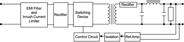 PSADF power supply block diagram
- Isolated topologies: Isolated topologies are required when you need isolation between input and output or between rails (for safety, regulatory, or noise reasons). For isolated converters, you must pay careful attention to transformer design, creepage/clearance, and routing between primary/secondary circuits.
- Hybrid approaches: e.g. an isolated primary converting to an internal bus, followed by several local non-isolated DC-DC regulators. This gives you the best of both isolation and efficiency.
Your ideal choice depends on input voltages, output rails, regulatory or safety requirements, and noise tolerance.
2. Power Integrity, PDN & Layout
A well-designed Power Delivery Network (PDN) is essential for PCB-based power supplies. This includes copper planes/traces, vias, decoupling, and careful layout so that voltage drop, ripple, and noise are kept acceptable across the board. Designers should:
- Use wide, low-impedance materials for high-current paths. A larger area and thickness will help lower any drops in voltage.
- Minimize loop areas for switching paths (e.g. input capacitor → switching node → inductor) to reduce EMI and stray inductance.
- Place decoupling and bypass capacitors close to regulators or loads with the shortest possible trace length. This helps avoid transients and maintain stability.
- Use multiple vias in parallel to carry heavy currents and to lower the via impedance.
- Manage ground return paths carefully. Signal ground and power ground may need to be tied at a defined point to avoid loops. Attention should be given to return paths and power planes.
- In multilayer boards, use internal planes for power and ground to help shield and supply low-impedance distribution.
3. Thermal Management & Heat Dissipation
PCB power supplies must be designed for thermal resilience to ensure reliability. This means regulating the amount of heat dissipated by the supply, while also designing features that lead to a wide operating temperature. Key practices include:
- Use thermal vias and heatsink pads under hot components to conduct heat into internal copper or to the board edge.
- Distributing high-power components rather than clustering them to avoid hot spots.
- Use board copper as a heat spreader. Wider planes help dissipate heat.
- Consider forced airflow if the ambient or board enclosure can’t suffice.
- Use temperature rating and derating factors to ensure components operate well within their thermal margins.
At Wall Industries, our PCB board power supplies undergo extensive testing to ensure wide storage and operating temperatures. One example is the PSAYC series, which features encapsulated models with a -40°C to +80°C operating temperature range.
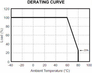 PSAYC series derating curve
4. Isolation, Safety, Creepage & Clearance Distances
Designers must take steps to ensure user safety when in proximity or direct contact with PCB systems. This is especially important in settings where the supply deals with hazardous mains voltages or outputs that require isolation, which can be common in medical electrical and electronic equipment (EEE) and industrial machinery. Recommendations include:
- Maintain creepage and clearance distances as per safety standards (e.g. IEC60950, IEC62368, or application-specific standards).
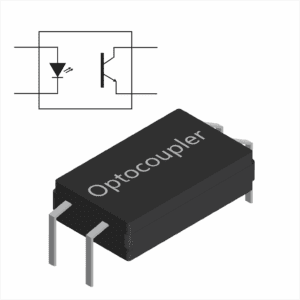
- Use isolation barriers (transformers, optocouplers) and ensure their insulation can withstand the required voltages.
- Keep primary and secondary routing separate, both physically and in terms of return paths.
- Use shielding or guard traces around switching nodes if needed.
- Clearly label and mark safety boundaries and high-voltage areas in manufacturing and assembly documentation.
5. EMI / EMC Mitigation & Filtering
PCB power supplies must have limits for conducted and radiated electromagnetic emissions, and be immune to electromagnetic noise from nearby equipment, meaning the layout of the supply plays a major role. Additionally, switching regulators are particularly known for generating high-frequency noise and require close attention. EMC mitigation includes:
- Input and output filters (LC, RC, common-mode chokes) to suppress conducted EMI.
- Snubber circuits or damping networks on switching nodes.
- Shielding or copper pours around noisy sections.
- Keeping analog, signal, or sensitive circuitry physically separated from switching nodes.
- Using differential routing where appropriate for noise immunity.
Our PSATC30 series meets the EN 55022 class B and EN 55024 standards for EMI and EMS (Noise Immunity), respectively. You’ll find similar protections across the Wall Industries product range, as our designers follow a thorough process in creating products which meet industry-specific standards and unique requirements.
6. Component Selection & Derating
Every component in the power supply must have the appropriate current, voltage, switching frequency, and thermal stats to meet the demands of the board. This includes inductors, capacitors, FETs, diodes, transformers, rectifiers, and cooling fans when present. Power supply designers should:
- Use components rated above the expected voltage/current (derating) to increase reliability.
- Select low-ESR capacitors for decoupling; use combinations (bulk + high-frequency) to cover broad spectral needs.
- Use MOSFETs or switching transistors with low Rds(on) and fast recovery diodes for efficiency.
- Transformers and inductors must have low leakage inductance and be suited for your switching frequency.
- Pay attention to part tolerances, aging, and long-term drift.
Application Areas & Sample Products Using PCB Power Supply Design
PCBs are widespread across many product types, from railway and telecommunications to medical devices and security systems. In almost all cases, these 3D printed circuit boards will require a power supply or power converter to ensure regular function. PCB-mount power supplies provide compact and efficient energy solutions in the following areas:
- Industrial controllers & automation boards – onboard DC-DC converters to supply power to logic and sensors.
- Robotics and motor control boards – onboard supplies deliver power to various components, including the PCB, which acts as the ‘nervous system’ of the robot.
- Telecom & networking equipment – on board DC-DC conversion from primary bus to module rails. Multiple output repeaters for wireless communications.
- Medical devices & patient monitoring – isolation, safety, and multiple rails for sensors, displays, and communications.
- IoT devices – compact power converter circuits embedded in system boards.
- Electric vehicle power modules / auxiliary supplies – integrated on main boards, which control various electronic features.
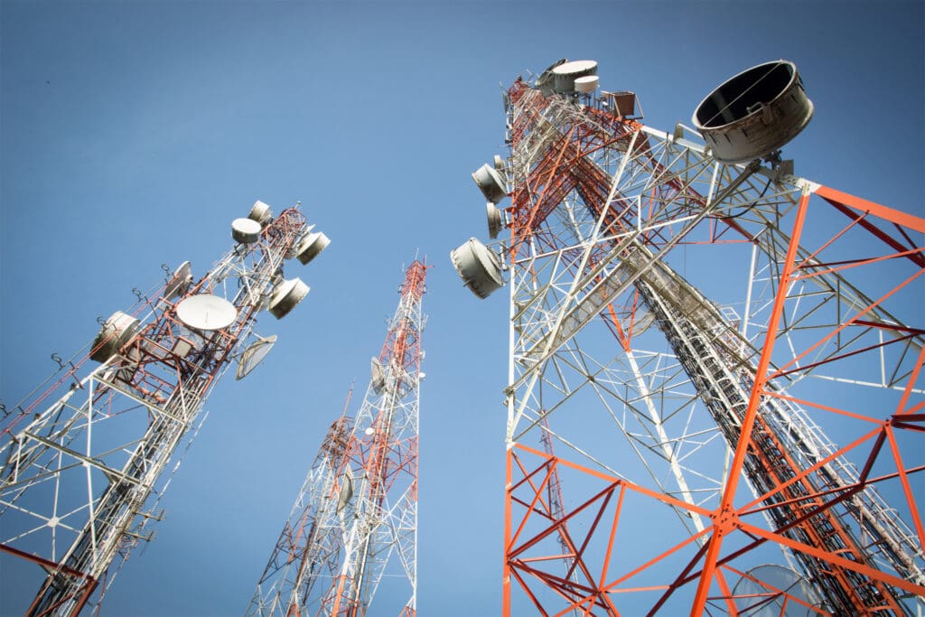
PCBs Offer Solutions in Wireless Communication Applications
Testing, Validation & Simulation
All power supplies must undergo various tests to determine whether they can demonstrate the right performance levels, protections, and meet relevant safety standards. These standards outline specific testing conditions for designers and manufacturers to follow. While you can use SPICE (Simulation Program with Integrated Circuit Emphasis) models to simulate tests in the early stages, prototypes will still need to be physically tested to prevent failures in post-production.
Tests for PCB power supplies can include:
- Burn-in testing and stress tests for reliability (over voltage, over power, and short circuit protection)
- EMI testing (IEC 61000, EN 55022)
- Humidity and ingress testing (IP rating)
- Safety approvals (CE, UL, cUL)
- Thermal imaging testing for efficiency
Need a Solution For Your Next Project?
Due to space constraints and industry requirements, designing a PCB power supply often requires balancing cost and complexity. Sourcing components with high tolerances and creating a compact power supply layout can consume more resources, but this will result in a more reliable power supply that can serve its intended purpose.
There are many factors to consider when choosing a power supply for a PCB, and as a result, you may not be able to find a perfect solution off the shelf. Our team can create a custom power supply that integrates seamlessly with your business’ infrastructure. This includes EMI requirements, wide operating temperatures, and compliance to specific standards such as MIL-STD-1275 and EN60601-1.
Get in touch to speak to a member of the Wall team about your ideal power solution.